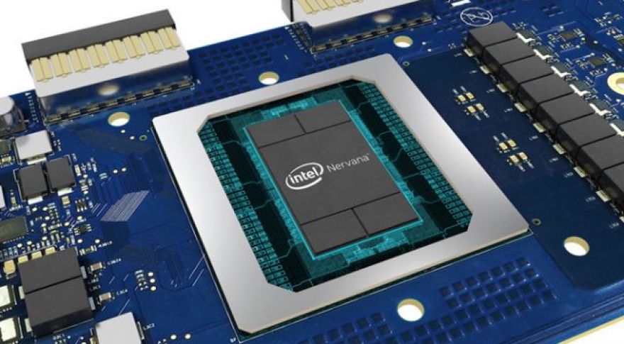
Intel Details Its Nervana Inference and Training AI Cards
Hot Chips 31 is underway this week, with presentations from a number of companies. Intel has decided to use the highly technical conference to discuss a variety of products, including major sessions focused on the company’s AI division. AI and machine learning are viewed as critical areas for the future of computing, and while Intel has tackled these fields with features like DL Boost on Xeon, it’s also building dedicated accelerators for the market.
The NNP-I 1000 (Spring Hill) and the NNP-T (Spring Crest) are intended for two different markets, inference and training. “Training” is the work of creating and teaching a neural network how to process data in the first place.
Intel’s Spring Crest NNP-T is designed to scale out to an unprecedented degree, with a balance between tensor processing capability, on-package HBM, networking capability, and on-die SRAMs to boost processing performance. The underlying chip is built by TSMC — yes, TSMC — on 16nm, with a 680mm2 die size and a 1200mm2 interposer. The entire assembly is 27 billion transistors with 4x8GB stacks of HBM2-2400 memory, 24 Tensor Processing Clusters (TPCs) with a core frequency of up to 1.1GHz. Sixty-four lanes of SerDes HSIO provides 3.58Tbps of aggregate bandwidth and the card supports an x16 PCIe 4.0 connection. Power consumption is expected to be between 150-250W. The chip was built using TSMC’s advanced CoWoS packaging (Chip-on-Wafer-on-Substrate), and carries 60MB of cache distributed across its various cores. CoWoS competes with Intel’s EMIB, but Intel has decided to build this hardware at TSMC rather than using its own foundries. Performance is estimated at up to 119 TOPS.
“We don’t want to waste die area on things we don’t need,” Intel VP of Hardware Carey Kloss told . “Our instruction set is simple; matrix multiply, linear algebra, convolutions. We don’t have registers per se, everything is a tensor (2D, 3D, or 4D).” There is a lot that is defined in software, including the ability to program the same when breaking a model to run on or off die. “Think of it as a hierarchy,” Kloss said in the interview. “You can use the same set of instructions to move data between two clusters in one group next to one HBM or between groups or even die in a network. We want to make it simple for software to manage the communication.”
The slideshow below steps through the NNP-T architecture. All data is courtesy of Intel, and the performance figures shared in the company’s microbenchmarks have obviously not been validated by ExtremeTech.


The NNP-T is designed to scale outwards effectively without requiring a chassis. Multiple NNP-T accelerators can be connected together in the same chassis, and the cards support chassis-to-chassis and even rack-to-rack glueless connection without needing a switch. There are four QFSP (Quad Small Form Factor Pluggable) network ports on the back of each mezzanine card.
We don’t have performance data yet, but this is the high-end training card Intel will come to market with to compete against the likes of Nvidia. It’s not yet clear how eventual solutions like Xe, which won’t ship for data centers until 2021, will fit into the company’s future product portfolio once it has both tensor processing cores and GPUs in the data center market.
Spring Hill / NNP-I: Icelake On-Board
Spring Hill, Intel’s new inference accelerator, is an entirely different beast. Where the NNP-T is designed for 150-250W power envelopes, the NNP-I is a 10-50W part intended to plug into an M.2 slot. It features two Icelake CPU cores paired with 12 Inference Compute Engines (ICE).
The 12 ICE engines and dual CPU cores are backed up by 24MB of coherent L3 and support both AVX-512 and VNNI instructions. There’s two on-die LPDDR4X memory controllers connected to an on-die pool of LPDDR4 memory (no word on capacity yet). DRAM bandwidth is up to 68GB/s, but total amount of on-card DRAM is unknown. Spring Hill can be added to any modern server that supports M.2 slots — according to Intel, the device communicates over the M.2 riser like a PCIe product rather than via NVMe.
The goal, with NNP-I, is to run operations on the AI processor with less overhead required from the primary CPU in the system. The device connects via PCIe (both PCIe 3.0 and 4.0 are supported) and handles the AI workload, using the on-die Icelake cores for any necessary processing. The on-die SRAMs and DRAM provide local memory bandwidth.
The Inference Compute Engine supports various instruction formats, ranging from FP16 to INT1, with a programmable vector processor and a 4MB SRAM for each individual ICE.
There’s also a tensor engine, dubbed the Deep Learning Compute Grid, and a Tensilica Vision P6 DSP (used for processing workloads that aren’t tuned for running in the fixed-function DL Compute Grid).
The overall memory subsystem of the NNP-I is also optimized, with the L3 cache broken into eight 3MB slices, shared between the ICE and CPU cores. The goal is to keep data as near to the processing elements that need it as possible. Intel claims the NNP-I can deliver ResNet50 performance of 3,600 inferences per second when running at a 10W TDP. That works out to 4.8 TOPS/watt, which meets Intel’s overall efficiency goals (the company claims that NNP-I is most efficient at lower wattages).
Intel doesn’t expect the NNP-I to come to the retail market, but inference solutions are doing a brisk business compared with the high-end data center-centric training solutions. The NNP-I could ship to a wide range of customers in the not-too-distant future, depending on overall uptake.
Both of these solutions are intended to challenge Nvidia in the data center. While they’re both quite different from Xeon Phi, you could argue that they collectively target some of the spaces Intel wanted to sell Xeon Phi into, albeit in very different ways. That’s not necessarily a bad thing, however — when the original Larrabee was built, the idea of using GPUs for AI and data center work was a distant concept. Revisiting the topic with a new specialized architecture for both inference and training is a smart move for Intel, if the company can grab volume away from Nvidia.
Now Read: